 Nanocavity-mediated Purcell enhancement of Er in TiO2 thin films grown via atomic layer deposition
ACS Nano (2024)
Erbium is commonly used in telecommunications devices and shows potential for applications in quantum communication. To scale up its use in larger quantum networks, it needs to be easily integrated into current photonics devices.
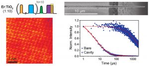
In this study, scientists at grew thin films of erbium-doped titanium dioxide on silicon. The researchers developed a growth process that kept the film’s surface smooth, crucial for integrating with nanophotonic devices.
After connecting these structures to high-quality resonators, the team found that the structures were able emit photons for longer stretches of time. This shows that the group’s method for growing erbium-doped thin films allows them to be easily integrated with silicon photonics — and may be used for on-chip amplifiers, lasers, or quantum memories.
The paper authors are Cheng Ji, Michael Solomon, Gregory Grant, Koichi Tanaka, Muchuan Hua, Jianguo Wen, Sagar Kumar Seth, Connor Horn, Ignas Masiulionis, Manish Kumar Singh, Sean E. Sullivan, F. Joseph Heremans, David Awschalom, Supratik Guha and Alan Dibos, who did their work at Argonne National Laboratory and the University of Chicago.