The Q-NEXT collaboration led the establishment two national quantum foundries to develop high-quality, standardized materials for quantum devices and systems. These resources provide an in-demand source of materials and data to accelerate progress across the National Quantum Information Science Research Centers and in national QIS research.
Quantum Foundries
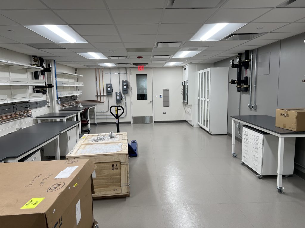
Argonne Quantum Foundry
Located at Argonne National Laboratory, the Argonne Quantum Foundry is a 6,000-square-foot facility focused on developing scalable semiconductor quantum systems. The foundry will be home to a quantum computing test bed. Other instruments to be co-located at the foundry are new diamond growth tools, environment-controlled annealing furnaces, tools to create qubits and materials transfer and flip-chip bonders for device integration.
Learn more, and view pictures of the foundry’s opening.
Spin qubit formation lab
Dedicated area for annealing furnaces, synthesis and defect activation tools. Annealing capabilities include a rapid thermal annealer, an ampule annealing furnace, and a vacuum furnace for qubit activation.
Qubit synthesis and preparation lab
Dedicated area for cutting and polishing diamond, silicon carbide and other solid-state systems, preparing them for growth synthesis and providing new avenues for device integration.
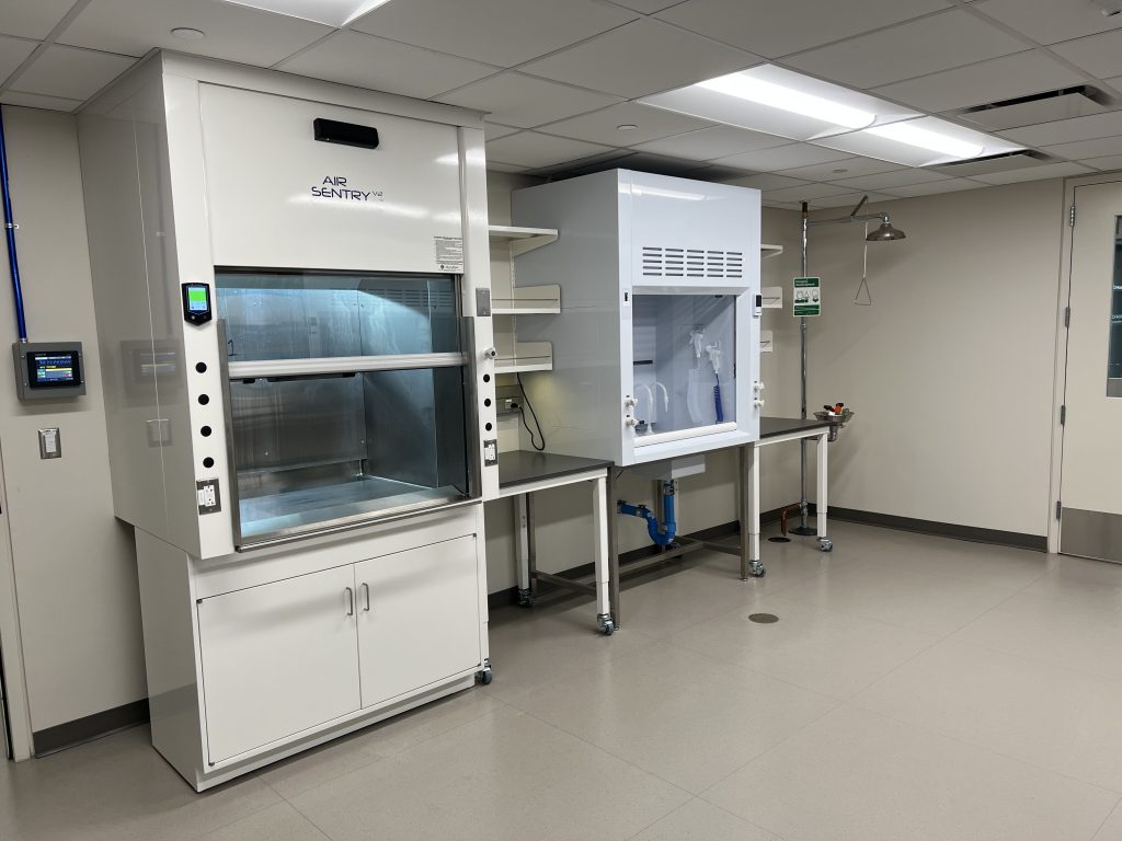
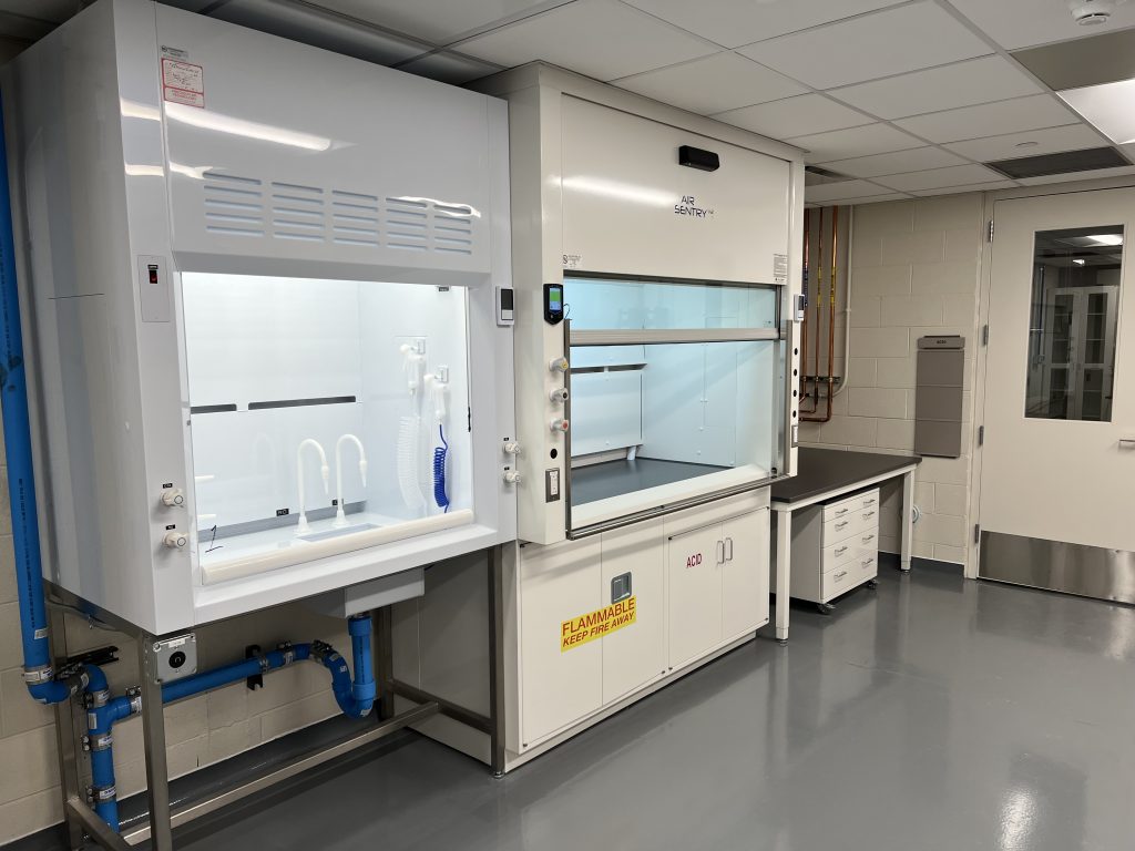
Surface treatment lab
Area equipped with sample cleaning and dedicated pechloric-acid-based tri-acid cleaning protocol for surface preparation of diamond and other solid-state hosts.
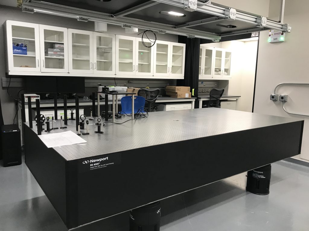
Optical processing and characterization lab
Optics lab dedicated to ultrafast pulsed lasers for local qubit creation and annealing.
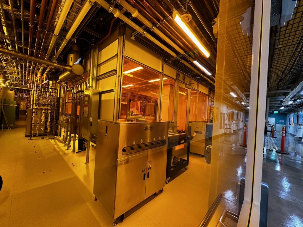
SLAC Detector Microfabrication Facility
The SLAC Detector Microfabrication Facility (DMF), located at SLAC National Accelerator Laboratory, is a 5,500-square-foot, class-100 cleanroom on the ground floor of the lab’s three-story Arrillaga Science Center. The facility, a superconducting quantum foundry, consists of a series of advanced equipment and metrology tools to support the state-of-the-art superconducting processes for a wide range of devices and sensors on 150-mm wafers. Facility capabilities include design, fabrication, and device characterization using cryogenic testing. The SLAC facility establishes methods and standards to improve the yield and robustness of superconducting processes to provide efficient, consistent, high-quality, and high-yield capabilities for superconducting quantum devices to support Q-NEXT and leverage other DOE missions.
Lithography bay cleanroom
This ISO 5 cleanroom in the lithography bay contains an ASML stepper, a Heidelberg laser direct write system, tracks, wet benches and related metrology tools.
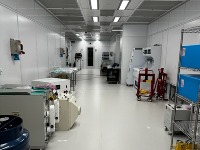
Main clean aisle
The main clean aisle connects six clean bays. Each bay accommodates a specific category of equipment and related metrology tools for device fabrication. Behind each door is a chase where supporting pumps, chillers and heat exchangers reside.