High-throughput spin-bath characterization of spin defects in semiconductors
Phys. Rev. Applied (2025)
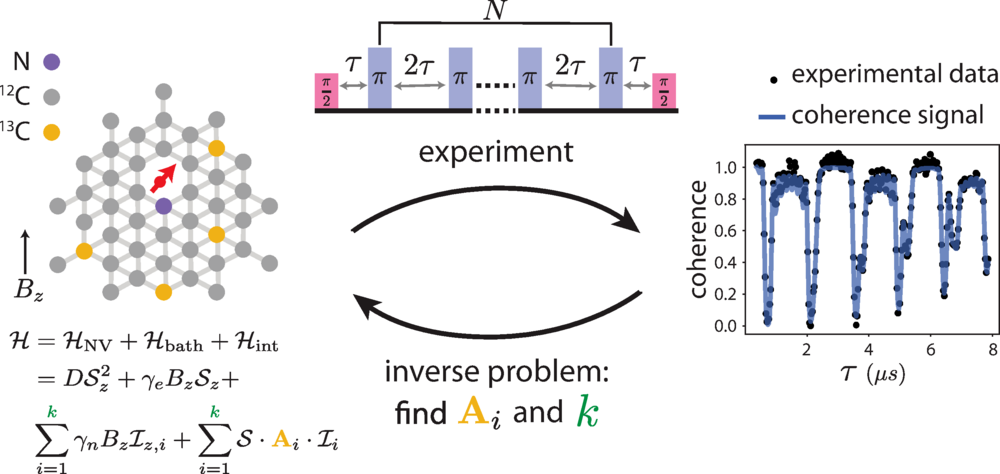
To use quantum defects in materials such as diamond or silicon carbide effectively, scientists need to understand the atomic environments around each defect. Today’s methods for measuring these environments are slow and hard to scale up because they require long, detailed experiments on each defect.
In this paper, researchers introduce new computer-based tools that can quickly and reliably reconstruct the positions and magnetic interactions of atoms near defects, using only short, noisy measurements that take hours instead of days. The approach uses Bayesian statistics and first-principles simulations to sort through noisy data and still recover accurate pictures of each defect’s environment.
The authors also provide guidelines for designing efficient experiments and show how their method can rapidly characterize many defects in practice. Together, this study enables faster, scalable use of spin defects for quantum sensing, quantum information, and even real-time “digital twin” models that can be updated as new data are collected.
The paper’s authors are Abigail Poteshman, Nikita Onizhuk, Christopher Egerstrom, Daniel Mark, David Awschalom, F. Joseph Heremans and Giulia Galli, who carried out this work at the University of Chicago and Argonne National Laboratory.