Katie Sautter is an architect of exquisite, invisible structures. Built one atomic layer at time, her team’s atomically engineered samples are the starting points for new materials that could one day enable a quantum network.
A postdoctoral researcher at the U.S. Department of Energy’s (DOE) Argonne National Laboratory, Sautter researches quantum materials as part of Q-NEXT, a DOE National Quantum Information Science Research Center established in 2020. The materials that emerge from her team’s research will be used in quantum communication devices.
“Quantum devices have an enormous range of potential applications in cybersecurity, computing, data communications, and lasers — quantum engineering can take all of these in a direction that can’t be taken using traditional methods,” said Sautter, who works with Q-NEXT in Argonne’s Nanoscience and Technology Division.
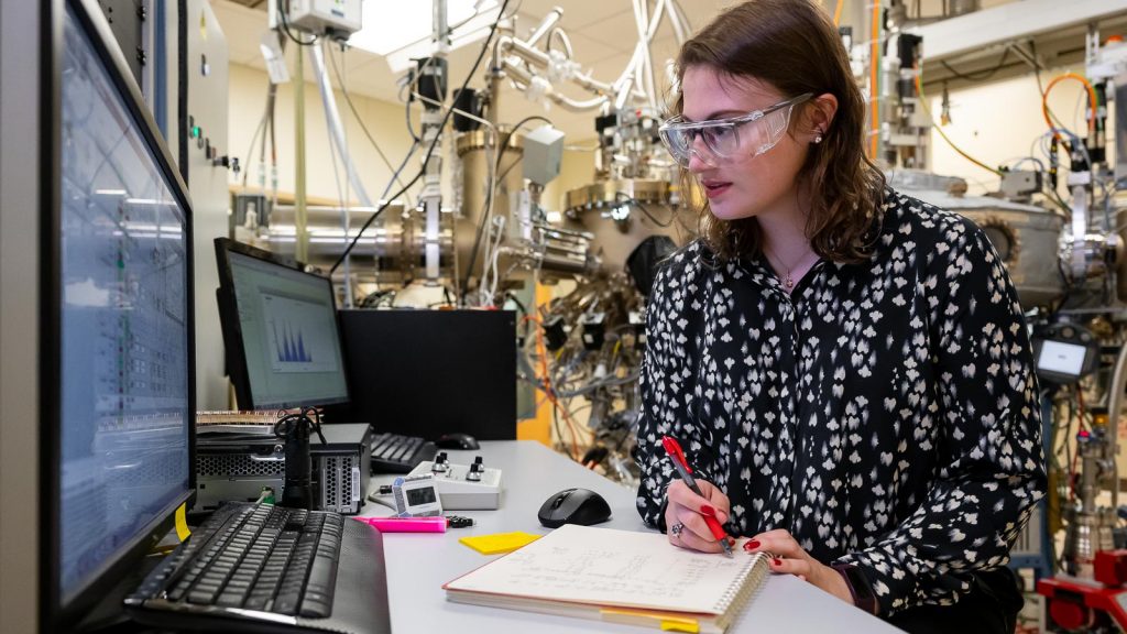
Sautter’s path to quantum engineering started at Pennsylvania State University, where she studied materials science and engineering following the advice of Jeffrey Brownson, a professor of engineering there. When the two first met, Sautter was part of a group of high schoolers touring the university. Brownson had been leading the group, and Sautter’s insightful questions caught his attention. After discussing her interests, Brownson gave her some career advice, and she enrolled at Penn State the following year, attracted by the quality of its materials science and engineering program, though she didn’t settle on a specialty immediately.
“It took me a while to find my path,” she said. “Then I interned at the National Renewable Energy Lab, working with the high-efficiency solar-cell team out there, and I loved it. That’s what inspired me to go for my Ph.D.” The National Renewable Energy Laboratory is a DOE national laboratory in Colorado.
Sautter received her Ph.D. in materials science and engineering in May 2021 from Boise State University, where she became an expert in a special material-growth process: Individual layers of atoms are meticulously stacked on top of one another using an instrument called a molecular beam epitaxy machine (MBE). She used the university’s MBE to make quantum dots, bits of matter only thousands of atoms wide. Five thousand dots could fit along the width of an average human hair.
Now a member of Q-NEXT, Sautter will help create materials for quantum memories that can be built on silicon chips, working under the guidance of Argonne scientist, University of Chicago Professor and Q-NEXT Chief Technology Officer Supratik Guha. If successful, these memories will be used in devices known as quantum repeaters.
“Materials science is awesome. We take what people have theorized and process it, feed it back to them, and reprocess it until we have a beautiful shiny thing. It’s the base on which everything else is built.” —Katie Sautter
Quantum repeaters enable the transmission of quantum information over longer distances of optical fiber. As the signal travels along the fiber, it weakens. The quantum repeater repeatedly “stitches” the signal back together so that the information can be conveyed along the fiber’s length. Without quantum repeaters, the signal could die before it arrives at its destination. Although quantum repeaters are only in the design stage, they hold great promise for quantum communication.
Researchers are also working to develop quantum memory devices that work in the telecommunication band of frequencies, making them compatible with today’s fiber-optic networks.
Such next-generation devices will need to be built from next-generation materials.
“We’re making brand new material structures that no one has ever made before, inventing something new that can be developed for these quantum devices,” Sautter said.
And to do that, she’ll use a specially designed MBE system in Guha’s laboratory, a steampunk-meets-scifi-looking tool that would fill a large bedroom.
“It looks like something out of Star Trek, like we have a warp drive inside our lab,” she said.
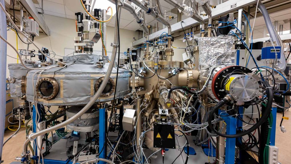
In MBE, different chemical elements are placed in separate compartments in the machine and heated. Like steam rising from a cup of tea, vapors rush away from the sources. Shutters allow the molecular puffs of vapor to pass out of the compartments and into a central chamber at precisely timed intervals.
The first gust of vapor to enter the chamber lands on a foundation, a wafer, creating the sample’s atom-thin first story. The next layer is quickly deposited on the first. So the process continues, with atomic layers piling up at rapid speed. Within one to three hours, the MBE builds enough material for a compact, high-performance device.
The result is a finely crafted molecular tower, an exquisite nanoscopic cake.
One of the advantages of MBE over comparable material-building processes is that it allows extreme control over the growth settings: The wafer temperature, the layering speed, and the deposition amounts can all be tuned to a T. By turning those knobs, the operator can ensure that, for example, every third layer is exactly 2 nanometers thick.
“That kind of precision with extreme cutoffs between layers — you could try to do it with something else, but it would be more difficult. MBE makes that process easy,” Sautter said. “The precision is immense.”
Shown here is one process for building a material one atomic layer at a time. It is similar to the process that will be used at the MBE in Supratik Guha’s lab for Q-NEXT research. This shows the growth of a gallium arsenide nanocrystal. (Image by Jean-Christophe Harmand and Gilles Patriarche, C2N-CNRS/University of Paris Saclay)
MBE also results in exceptionally pure materials. Other processes use certain chemicals to jump-start the production of the desired end-product. And while the initial compounds are not meant to be part of the final mix, they sometimes end up there anyway. MBE dispenses with such preparatory compounds for the most part, avoiding sample contamination.
Sautter enjoys the nitty-gritty nature of molecular beam epitaxy.
“It’s kind of an intense tool, and it can take years to learn,” Sautter said. “If you can wrangle a difficult one, like I did at Boise State, whose machine was from 1992, you can probably wrangle a newer, more refined or more automatic machine. I’ve been told that the MBE is one of the hardest tools to learn in science because it has so many components.”
Sautter and her team in Guha’s lab will focus on building oxide heterostructures – materials with layers made of two or more oxygen compounds. Their particular structural arrangements and the way they interact with their surroundings make them ideal for quantum memory processing.
“Materials science is awesome. We take what people have theorized and process it, feed it back to them, and reprocess it until we have a beautiful shiny thing. It’s the base on which everything else is built,” Sautter said. “It’s pretty satisfying science.”
Now she’s using that science to advance another.
“I’m excited to be doing MBE in something similar but different from my Ph.D. and on a fancy new machine,” she said. “Quantum information science is going to change the planet. It helps everyone.”
This work was supported by the DOE Office of Science National Quantum Information Science Research Centers.